| Issue |
Res. Des. Nucl. Eng.
Volume 2, 2026
|
|
|---|---|---|
| Article Number | 2026001 | |
| Number of page(s) | 7 | |
| DOI | https://doi.org/10.1051/rdne/2026001 | |
| Published online | 12 May 2026 | |
Interfacial electronic and energetic evaluation using perturbation-resolved spectrometrics for nuclear radiation resistance
1
Research Institute of Interdisciplinary Sciences (RISE) and School of Materials Science & Engineering, Dongguan University of Technology, Dongguan 523808, Guangdong, PR China
2
College of Engineering, Nanyang Technological University, Singapore 659798, Singapore
* e-mail: This email address is being protected from spambots. You need JavaScript enabled to view it.
Received:
11
July
2025
Accepted:
2
April
2026
Abstract
Based on perturbation-resolved electron spectrometrics (PRS), we derived that the radiation resistance of hetero-juncted interfaces is fundamentally predetermined by their static, ground-state electronic structure, not merely by dynamic atomic collision events. Interfaces dominated by charge polarization (CP), like Be/W (γ < 1), act as “electronic sponges,” efficiently dissipating incident energy via non-destructive electronic stopping before atomic displacements occur. The γ-factor quantifies the deviation of interfacial potential depth from the isolated constituent of the alloy, linking quantum characteristics to macroscopic performance. Conversely, quantum entrapment (QT)-dominant, such as Cu/Sn (γ > 1), localizes energy into the lattice. CP-dominant Be/W exhibits an energy density of 101.25 eV/Å3 – nearly four times higher than QT-dominant Cu/Sn (27.07 eV/Å3). This electronic polarization and high-energy density predetermination explain the superior radiation tolerance of Be/W-based alloys in fusion environments. The work shifts radiation damage paradigms from reactive defect models to proactive quantum-level design, enabling engineered materials for extreme environments.
Key words: Radiation / Hetero-interface / Quantum Entrapment / Charge Polarization / XPS
© The Author(s) 2026. Published by EDP Sciences.
 This is an Open Access article distributed under the terms of the Creative Commons Attribution License (https://creativecommons.org/licenses/by/4.0), which permits unrestricted use, distribution, and reproduction in any medium, provided the original work is properly cited.
1 Introduction
The pursuit of clean and virtually limitless energy through nuclear fusion is a grand challenge to mankind whose resolution is fundamental to reshaping the future energy landscape [1, 2]. The success of endeavors like ITER [3, 4], however, is not merely a plasma physics challenge; it is fundamentally limited by materials science: developing materials capable of withstanding unprecedented radiation fluxes at their structural interfaces [5–7]. For decades, the dominant conceptual framework for understanding and predicting radiation damage has been rooted in classical ballistics, focusing on the dynamic cascade of atomic displacements initiated by high-energy particles [8, 9]. While this “event-driven” model remains foundational, it is inherently blind to the pre-existing electronic ground state that governs primary energy dissipation, thus proving insufficient to predict the starkly different fates of advanced materials under irradiation, leaving the design of truly radiation-resilient materials largely to empirical trial-and-error.
This limitation is most acute at the hetero-coordinated interface – the precise junction where dissimilar materials meet and where performance is ultimately decided [10–12]. It is here that experimental observations present a profound conundrum: some interfaces exhibit remarkable resilience, while others, with seemingly similar compositions, fail catastrophically under irradiation [6, 13, 14]. For instance, under irradiation doses, helium bubble volume fractions in the Be/W interface region remain below 2% [15]. This dramatic difference in defect accumulation directly leads to disparate mechanical responses; post-irradiation nanoindentation reveals that the hardening in W grain is a 0.34 GPa (7.11–7.45 GPa), while Cu-based intermetallics can become catastrophically brittle, exhibiting hardening up to 1.9, 1.8, 1.4 GPa for single crystal Cu, 70 nm Cu/Nb, 5 nm Cu/Nb multilayers respectively after 7 at.% implantation [16]. Clues to the origin of this vast disparity in performance lie in the electronic structure; spectroscopic measurements have long detected anomalous core-level shifts at these interfaces, suggesting a fundamental underlying electronic mechanism [17]. Yet, these have remained isolated observations. The field has lacked a unifying physical principle to answer a fundamental and critical question: Does the interface’s static, pre-existing electronic ground state – its intrinsic quantum-mechanical nature – actively determine its ultimate behavior under irradiation?
Here, we propose an alternative to the conventional model, shifting from a view focused on reactive damage events to one centered on deterministic material properties. We hypothesize that an interface’s tolerance is not an outcome of random collisional events but is intrinsically governed by its ground-state electronic bonding [18–20]. This principle manifests as two distinct mechanistic pathways [19]: interfaces dominated by quantum entrapment (QT) localize electronic states, which channel incident energy into localized, high-amplitude lattice vibrations. Conversely, those governed by charge polarization (CP) feature a delocalized electronic system that can rapidly dissipate incident energy through non-destructive electronic channels, effectively dissipating the energy before it can couple to the atomic lattice and trigger damage. To validate such a principle, however, requires a method capable of quantifying this governing electronic signature and directly linking it to the material’s macroscopic energy dissipation capacity.
In this communication, we present a theoretical and experimental framework that provides the unified physical basis for a wide range of previously disparate experimental findings on radiation damage. This is achieved by developing and applying a perturbation-resolved spectrometric (PRS) technique [18, 21, 22] that parameterizes abstract quantum states through a physical quantity of interfacial potential, the γ-factor. Using this, we quantitatively classify the interfacial bonding character of three prototypical systems reported in the literature, revealing the contrast between the CP-dominant Be/W interface [23, 24] (γ < 1), the QT-dominant Cu/Sn interface (γ > 1), and the CP and QT mixture of Si/C.
Crucially, our analysis demonstrates that this microscopic electronic signature fundamentally determines the macroscopic damage initiation threshold, explaining the nearly four-fold higher energy density calculated for the resilient Be/W system (101.25 eV/Å3) compared to the Cu/Sn system (27.07 eV/Å3). These findings are consistent with the significant performance differences highlighted earlier, and numerous other previously unexplained experimental phenomena. This study suggests a predictive, quantum-based principle, shifting the materials design concept from post-failure analysis to the a priori engineering of materials from the level of electronic structure for the most extreme environments.
2 Methods
2.1 Principles: tight-binding theory
2.1.1 Energy band formation
When atoms condense into a solid, the interatomic interactions shift the discrete atomic energy levels and widen them into energy bands. For a solid with N atoms, each atomic level splits into N sublevels, forming continuous energy bands (e.g., valence band, conduction band, and core bands), if N is sufficiently large. This band structure governs electronic behavior, with the Fermi level (EF) separating occupied and unoccupied states. The work function (φ = E0 − EF) dictates the ease of electron ejection. In contrast, the electron affinity (energy from the vacuum level E0 to the conduction band minimum) determines the capacity for electron capture. The electronegativity difference between elements defines the nature of the interatomic bond and charge-sharing dynamics.
2.1.2 Band hierarchy and energy shifts
The conduction band (CB) houses delocalized electrons of a conductor, but remains unoccupied in semiconductors at 0 K. In contrast, the slightly deeper valence band (VB) contains bonded electrons and is fully occupied in semiconductors. The even deeper core bands (CL) are accommodated by localized inner-shell electrons, exhibiting minimal dispersion upon purbation – CL shift alongside band broadening.
The center of each CL shifts from the E(0) of an isolated atom downward proportionally to bond energy (Eb) at equilibrium when subjecting to solid formation or external perturbation (coordination imperfection, electrification, mechanical and thermal activation, etc.), according to the Tight-binding theory [25]. The Hamiltonian H = H0 + Vcryst(r) describes electron dynamics, where H0 is the Hamiltonian of an isolated atom including electronic kinetic energy and the interatomic potential energy, and Vcryst sums interatomic potentials over the neighboring atoms of a specific atom. Bulk (B with full coordination zb), atomic undercoordination (z) and alloy hetero-coordination interface (I) bonding modulate the νth CLS through perturbing Vcryst(I):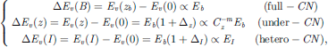 (1)
(1)
where Cz = 2/[1 + exp[(12 − z)/(8z)]] is the bond length contraction coefficient, and m is the bond nature index, correlating the bond energy and length E(z) = Cz−mEb for the undercoordinated systems including defects, surfaces, and nanostructures [18]. Index I and B denote the interface heterocoordination effect and B the bulk reference. Δz and ΔI denote the Hamiltonian perturbation by the respective atomic under- and heterocoordination effects. Band modifications via heterocoordination tune the electron energy density landscapes for tailored nuclear shielding, leveraging entrapment for enhanced attenuation or polarization for reduced secondary emissions.
2.1.3 Irregular-coordination effects
Atomic undercoordination (defects, surfaces, nanostructures) and hetero-coordination (alloys, interfaces, dopants, compounds) perturb the band structure through Hamiltonian [18]:
Undercoordination (BOLS-NEP): Bond order loss shortens/strengthens bonds (bond contraction coefficient Cz), densifying charge and deepening local potentials (Fig. 1a), leading to:
- ◦
Quantum entrapment (QT): Positive core-level shift (CLS) because of bond strengthening.
- ◦
Polarization (CP): Negative shift of valence electrons.
- ◦
Hetero-coordination (entrapment/polarization): alters bond nature with A–B type bond involvement, creating an interface potential well/barrier, see Figure 1b, resulting in
- ◦
QT dominance: γ = Vcryst(I)/Vcryst(B) = 1+ ΔH > 1.
- ◦
CP dominance: γ < 1.
- ◦
 |
Fig. 1 Illustration of (a) atomic undercoordination induced surface bond contraction (Cz) and potential-well quantum entrapment (QT), and (b) heterocoordination induced interface bond nature alteration and potential well/barrier formation with γ = Vcryst(r, I)/Vcryst(r, B) being the well depth (γ > 1, QT dominance) or barrier height (γ < 1, charge polarization (CP) dominance). (c) Irregular coordination effects on the CL shift from the E(0) to E(B) upon bulk formation and further shift under perturbation. Reprinted with permission from [26, 27]. Copyright 2014, 2020, Springer-Verlag. |
XPS probes directly the CLS from the Eν(0) of an isolated atom to the bulk value of Eν(B) and then further upon perturbation, e.g., surface or interface formation, as illustrated in Figure 1c. The Eν(0) and Eν(B) values are independent of the type or degree of an applied perturbation. The CL bandwidth narrows progressively from VB to deeper core bands (e.g., 100 eV for VB to 10−1 eV for deep cores because of the screen shielding of electrons in the outer orbitals).
2.2 Perturbation-resolved spectrosmetrics (PRS)
Alloys can be made by thermal annealing of samples continuously deposited on a substrate to ensure sufficient interfacial diffusion and bond formation. Core-level shift (CLS) giving rise to information of bond energy gain can be probed using light sources of Al Kα (hν = 1486.6 eV), Mg Kα (1253.6 eV), or synchrotron radiation, by measuring the kinetic energy (EK) of electron ejected from the νth core band. Calculate binding energy (EB) based on the principle of Einstein’s opto-electronic effect: (2)where hν is the photon energy and ϕ is the work function.
Collecting at least two spectra from a certain energy level of each constituent of the AB alloy before and after annealing or sufficient diffusion, the PRS is performed by subtracting the specific spectral peak of the pristine constituent from the conditioned (e.g., alloyed) fone of to extract information due to interface interaction, upon all of them being peak area normalized to minimize electron scattering artifacts. The residual density-of-states (Δg(E)) and the center-of-gravity of energy (ECOG) describe the energy transition from the pristine element to the interfaces: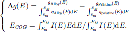 (3)The PRS avoids the experience-based peak deconvolution, providing direct information about the g(E) transition and PRS peak energy.
3 Results and discussion
3.1 PRS: core band entrapment and polarization
Irregular coordination directly modulates local bond strain and energetics (bond energy, energy density, and atomic cohesive energy) [18], thereby governing mechanical strength, thermal stability, chemical reactivity, and nuclear radiation resistance. By applying PRS to the XPS spectra, one can directly extract the interfacial bond energy EI and determine whether QT or CP governs interfacial behavior. One can calculate critical parameters such as interfacial binding-energy density EID, atomic cohesive energy EIC, and free energy ΓI, enabling quantitative assessment of interface energetics.
Figure 2 shows the PRS for Si/C, Be/W, and Cu/Sn alloys. Si/C shows a mixture of QT (Si 2p3/2) and CP (C 1s), both Be 1s and W 4f7/2 of Be/W manifest CP dominance, while Cu 2p3/2 and Sn 3d3/2 show QT dominance. Table 1 summarizes information extracted from PRS measurements.
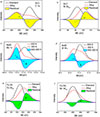 |
Fig. 2 XPS CL shift and intensity inversion upon interface hetero-coordinated atomic diffusion of (a, b) Si/C (C 1s polarization and Si 2p3/2 entrapment), (c, d) Be/W (Be 1s and W 4f7/2 polarization), and (e, f) Cu/Sn (Cu 2p3/2 and Sn 3d3/2 entrapment; XPS data are sourced from [23] for Be/W. |
The interfacial CP weakens the C–C bond by 1 – γ = 89% while strengthening the Si–Si by 40%. The Be–Be and W–W bond weakens by 24% and 29%, respectively. In contrast, the interfacial Cu–Cu and Sn–Sn bonds are enhanced by 66% and 17%, respectively.
For an alloy containing N constituent elements, there will be C(N,2) terms of interactions, such as the A–A, B–B, and A–B interactions for an AB alloy instance. The additional A–B type exchange interactions contribute to the overall potential of the alloy. Understanding the fundamental nature of the interface bond formation and its consequence on the electronic BE shifting, as well as the determination of the relevant energetics, is necessary.
Spectrometric information on the νth CL shift from an isolated atom Eν(0) to its bulk Eν(B) and interface formation Eν(I) (in eV unit) and their relative shift (bond energy) γ = ΔEν(I)/ΔEν(B) =[Eν(I) − Eν(0)]/[Eν(B) − Eν(0)] for Si/C, Be/W, and Cu/Sn interfaces.
3.2 Interfacial energetics
One can estimate the interfacial energy density EID, atomic cohesive energy EIC, and the free energy ΓI based on the PRS-derived interface potential depth γ. The EID is the sum of BE per unit cell. The EIC is the sum of BE over all coordinates of an interface atom. Instead of the conventionally defined excessive energy required for creating a unit area of interface, ΓI equals the division of EID by the mean cross-sectional area of the interface atoms.
For simplicity, the interfaces are assumed to hold the diamond structure for Si/C, fcc for Cu/Sn, and bcc for Be/W. Atoms in the interface region are fully coordinated with zI = 4, 12, and 8. The following determines the mean interface bond energy 〈EI〉: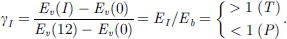 (4)Vegard’s notion expresses the mean interface bond energy 〈EIS〉 and bond length 〈dIS〉 with the involvement of the A–A, B–B, and A–B type interactions [33]:
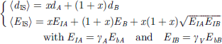 (5)The last term in the 〈EIS〉 denotes the A–B exchange interaction and x = 1/2 the alloy concentration. With the derived 〈dIS〉 and 〈EIS〉, we can determine the interfacial energetics (EID, EID, and ΓI):
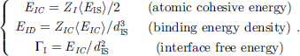 (6)These quantities are different from those of the corresponding bulk constituent because of the involvement of interface exchange coupling. As given in Table 2, the EID of the Be/W interface is the highest among the three, which justifies that the Be/W becomes an important medium for radiation resistance due to its higher energy density and interface electron polarization.
PRS revealed the interface QT dominance of Cu/Sn and Si in Si/C, while CP is dominant in Be/W alloy and C in SiC. The QT creates holes at the upper edge of the valence band, serving as a charge acceptor in the process of catalytic reaction. The CP dominance of Be/W generates excessive electrons at the upper conduction band edge, serving as a charge donor in the reaction. The electron polarization and the high interface energy density explain why the Be/W can protect against nuclear radiation.
Interface mean bond energy 〈EIS〉, mean lattice constant 〈dIS〉, energy density EID, and the free energy ΓI. Eb and db are the bond energy and bond length of the constituent bulk reference, respectively. EI(A–A or B–B) is the bond energy of A or B in the interface; EI(A–B) is the A–B exchange interaction energy [10, 19, 32, 34] (length in nm and energy in eV unit unless indicated).
4 Conclusion
In conclusion, this work has unequivocally demonstrated that the radiation resistance of a hetero-interface is decisively pre-determined by its static, ground-state electronic structure. By establishing a spectrometric methodology to directly quantify the interfacial potential (γ-factor), we have built a quantitative bridge between the quantum-mechanical cause and its macroscopic energetic consequence. The clear distinction between the “flexible” CP-dominant Be/W interface (γ < 1) and the “rigid” QT-dominant Cu/Sn interface (γ > 1) translates directly into a nearly four-fold disparity in their energy-bearing capacity, providing a deterministic Si/C basis for their widely divergent radiation damage behaviors, though the Si/C has not been used in radiation protection. This work fundamentally shifts the perspective of radiation damage science from a reactive, defect-centric viewpoint to a proactive, predictive one based on ground-state quantum chemistry. The principle of “electronic pre-determination” offers a powerful and universal design strategy, paving the way for the rational, a priori design of a new generation of ultra-resilient materials for nuclear fusion, aerospace, and other extreme environments where performance is dictated at the quantum level.
Funding
Support from the Guangdong Provincial (No. 2024A1515011094(CQ)) is gratefully acknowledged.
Conflicts of interest
The authors declare no competing financial interest.
Data availability statement
No additional data is associated with the work
Author contribution statement
CQS conceived the project and write the article. YZ and LHM analysed the experimental data, BW reviewed the manuscript.
References
- M.R. Abdussami, A. Verma, Future energy landscapes: Analyzing the cost-effectiveness of nuclear-renewable integrated energy Systems in Retrofitting of coal power plants, Appl. Energy 377, 124460 (2025). [Google Scholar]
- B. Fattouh, S. Vakhshouri, J. Henderson, Nuclear energy in the global energy landscape: advancing sustainability and ensuring energy security? in Oxford Energy Forum: A Quarterly Journal for Debating Energy Issues and Policies (The Oxford Institute for Energy Studies, Oxford, 2024). [Google Scholar]
- K. Fiore, Nuclear energy and sustainability: Understanding ITER, Energy Policy 34, 3334–3341 (2006). [Google Scholar]
- S. Geng, An overview of the iter project, in J. Phys. Conf. Ser. (IOP Publishing, 2022), p. 012012. [Google Scholar]
- I. Beyerlein, A. Caro, M. Demkowicz, N. Mara, A. Misra, B. Uberuaga, Radiation damage tolerant nanomaterials, Mater. Today 16, 443–449 (2013). [Google Scholar]
- Z. Su, H. Jiang, H. Li, Y. Zhang, J. Chen, J. Zhao, Y. Ma, Recent progress on interfaces in nanomaterials for nuclear radiation resistance, ChemNanoMat 9, e202200477 (2023). [Google Scholar]
- T. Vogl, K. Sripathy, A. Sharma, P. Reddy, J. Sullivan, J.R. Machacek, L. Zhang, F. Karouta, B.C. Buchler, M.W. Doherty, Radiation tolerance of two-dimensional material-based devices for space applications, Nature Commun. 10, 1202 (2019). [Google Scholar]
- M.T. Robinson, Basic physics of radiation damage production, J. Nucl. Mater. 216, 1–28 (1994). [Google Scholar]
- K. Nordlund, S.J. Zinkle, A.E. Sand, F. Granberg, R.S. Averback, R.E. Stoller, T. Suzudo, L. Malerba, F. Banhart, W.J. Weber, Primary radiation damage: A review of current understanding and models, J. Nucl. Mater. 512, 450–479 (2018). [Google Scholar]
- Z.S. Ma, Y. Wang, Y.L. Huang, Z.F. Zhou, Y.C. Zhou, W.T. Zheng, C.Q. Sun, XPS quantification of the hetero-junction interface energy, Appl. Surf. Sci. 265, 71–77 (2013). [Google Scholar]
- C.Q. Sun, Relaxation of the chemical bond: Skin chemisorption size matter ZTP mechanics H2O Myths (Springer-Verlag, 2014). [Google Scholar]
- C.Q. Sun, Electron and phonon spectrometrics (Springer-Nature, 2020). [Google Scholar]
- M. Demkowicz, P. Bellon, B. Wirth, Atomic-scale design of radiation-tolerant nanocomposites, MRS Bull. 35, 992–998 (2010). [Google Scholar]
- V. Shutthanandan, S. Choudhury, S. Manandhar, T.C. Kaspar, C. Wang, A. Devaraj, B.D. Wirth, S. Thevuthasan, R.G. Hoagland, P.P. Dholabhai, Radiation tolerant interfaces: Influence of local stoichiometry at the misfit dislocation on radiation damage resistance of metal/oxide interfaces, Adv. Mater. Interf. 4, 1700037 (2017). [Google Scholar]
- M. Baldwin, R. Doerner, Helium induced nanoscopic morphology on tungsten under fusion relevant plasma conditions, Nucl. Fusion 48 (2008) 035001. [Google Scholar]
- N. Li, M. Nastasi, A. Misra, Defect structures and hardening mechanisms in high dose helium ion implanted Cu and Cu/Nb multilayer thin films, Int. J. Plast. 32, 1–16 (2012). [Google Scholar]
- M. Khanuja, B. Mehta, S. Shivaprasad, Geometric and electronic changes during interface alloy formation in Cu/Pd bimetal layers, Thin Solid Films 516, 5435–5439 (2008). [Google Scholar]
- X.J. Liu, X. Zhang, M.L. Bo, L. Li, Y.G. Nie, H. Tian, Y. Sun, S. Xu, Y. Wang, W. Zheng, C.Q. Sun, Coordination-resolved electron spectrometrics, Chem. Rev. 115, 6746–6810 (2015). [Google Scholar]
- C.Q. Sun, Y. Wang, Y.G. Nie, B.R. Mehta, M. Khanuja, S.M. Shivaprasad, Y. Sun, J.S. Pan, L.K. Pan, Z. Sun, Interface quantum trap depression and charge polarization in the CuPd and AgPd bimetallic alloy catalysts, Phys. Chem. Chem. Phys. 12, 3131–3135 (2010). [Google Scholar]
- G. Dong, Y. Wang, W. Jiang, Y. Zou, Z. Ma, Interface adhesion properties characterization of sulfide electrode materials by the combination of BOLS and XPS, Sci. China Technol. Sci. 65, 1798–1807 (2022). [Google Scholar]
- C.Q. Sun, Y. Huang, X. Zhang, Z. Ma, B. Wang, The physics behind water irregularity, Phys. Rep. 998, 1–68 (2023). [Google Scholar]
- Y. Zhou, L. Li, Y. Huang, J. Ou, W. Li, H. Fang, C.Q. Sun, B. Wang, Perturbative vibration of the coupled hydrogen-bond (O: H–O) in water, Adv. Colloid Interf. Sci. 310, 102809 (2022). [Google Scholar]
- A. Wiltner, C. Linsmeier, Surface alloying of thin beryllium films on tungsten, New J. Phys. 8, 181 (2006). [Google Scholar]
- C. Linsmeier, K. Ertl, J. Roth, A. Wiltner, K. Schmid, F. Kost, S. Bhattacharyya, M. Baldwin, R. Doerner, Binary beryllium–tungsten mixed materials, J. Nucl. Mater. 363, 1129–1137 (2007). [Google Scholar]
- M.A. Omar, Elementary solid state physics: principles and applications (Addison-Wesley, New York, 1993). [Google Scholar]
- C.Q. Sun, Relaxation of the chemical bond: skin chemisorption size matter ZTP mechanics H2O myths (Springer-Verlag 2014). [Google Scholar]
- C.Q. Sun, Electron and phonon spectrometrics (Springer-Nature, 2020). [Google Scholar]
- C.Q. Sun, Y. Sun, Y.G. Nie, Y. Wang, J.S. Pan, G. Ouyang, L.K. Pan, Z. Sun, Coordination-resolved C-C bond length and the C 1s binding energy of carbon allotropes and the effective atomic coordination of the few-layer graphene, J. Phys. Chem. C 113, 16464–16467 (2009). [Google Scholar]
- C.Q. Sun, L.K. Pan, Y.Q. Fu, B.K. Tay, S. Li, Size dependence of the 2p-level shift of nanosolid silicon, J. Phys. Chem. B, 107, 5113–5115 (2003). [Google Scholar]
- Y. Wang, Y.G. Nie, J.S. Pan, L. Pan, Z. Sun, C.Q. Sun, Layer and orientation resolved bond relaxation and quantum entrapment of charge and energy at Be surfaces, Phys. Chem. Chem. Phys. 12, 12753–12759 (2010). [Google Scholar]
- Y.G. Nie, X. Zhang, S.Z. Ma, Y. Wang, J.S. Pan, C.Q. Sun, XPS revelation of tungsten edges as a potential donor-type catalyst, Phys. Chem. Chem. Phys. 13, 12640–12645 (2011). [Google Scholar]
- Y. Wang, Y. Pu, Z. Ma, Y. Pan, C.Q. Sun, Interfacial adhesion energy of lithium-ion battery electrodes, Extreme Mech. Lett 9, 226–236 (2016). [Google Scholar]
- L. Vegard, H. Schjelderup, Constitution of mixed crystals, Physik. Z, 18, 93–96 (1917). [Google Scholar]
- Y. Nie, Y. Wang, X. Zhang, J. Pan, W. Zheng, C.Q. Sun, Catalytic nature of under- and hetero-coordinated atoms resolved using zone-selective photoelectron spectroscopy (ZPS), Vacuum, 100, 87–91 (2014). [Google Scholar]
- C. Kittel, Introduction to Solid State Physics, 8 ed. (John Willey & Sons, Inc, New York, 2005). [Google Scholar]
Cite this article as: Sun CQ, Zhou Y, Ma L & Wong B. Interfacial electronic and energetic evaluation using perturbationresolved spectrometrics for nuclear radiation resistance. 2, 2026001 (2026), https://doi.org/10.1051/rdne/2026001.
All Tables
Spectrometric information on the νth CL shift from an isolated atom Eν(0) to its bulk Eν(B) and interface formation Eν(I) (in eV unit) and their relative shift (bond energy) γ = ΔEν(I)/ΔEν(B) =[Eν(I) − Eν(0)]/[Eν(B) − Eν(0)] for Si/C, Be/W, and Cu/Sn interfaces.
Interface mean bond energy 〈EIS〉, mean lattice constant 〈dIS〉, energy density EID, and the free energy ΓI. Eb and db are the bond energy and bond length of the constituent bulk reference, respectively. EI(A–A or B–B) is the bond energy of A or B in the interface; EI(A–B) is the A–B exchange interaction energy [10, 19, 32, 34] (length in nm and energy in eV unit unless indicated).
All Figures
|
Fig. 1 Illustration of (a) atomic undercoordination induced surface bond contraction (Cz) and potential-well quantum entrapment (QT), and (b) heterocoordination induced interface bond nature alteration and potential well/barrier formation with γ = Vcryst(r, I)/Vcryst(r, B) being the well depth (γ > 1, QT dominance) or barrier height (γ < 1, charge polarization (CP) dominance). (c) Irregular coordination effects on the CL shift from the E(0) to E(B) upon bulk formation and further shift under perturbation. Reprinted with permission from [26, 27]. Copyright 2014, 2020, Springer-Verlag. |
| In the text | |
|
Fig. 2 XPS CL shift and intensity inversion upon interface hetero-coordinated atomic diffusion of (a, b) Si/C (C 1s polarization and Si 2p3/2 entrapment), (c, d) Be/W (Be 1s and W 4f7/2 polarization), and (e, f) Cu/Sn (Cu 2p3/2 and Sn 3d3/2 entrapment; XPS data are sourced from [23] for Be/W. |
| In the text | |
Current usage metrics show cumulative count of Article Views (full-text article views including HTML views, PDF and ePub downloads, according to the available data) and Abstracts Views on Vision4Press platform.
Data correspond to usage on the plateform after 2015. The current usage metrics is available 48-96 hours after online publication and is updated daily on week days.
Initial download of the metrics may take a while.